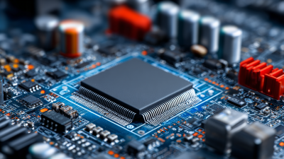
Common Challenges in PCB Board Design: Overcoming Technical and Operational Hurdles
In the rapidly evolving field of electronics, the significance of
effective PCB board design
cannot be overstated. According to a report by Research and Markets, the global PCB market is projected to reach
$80 billion by 2025, driven by advancements in technology and increasing demand for miniaturized electronic devices.
However, despite the industry's growth, many engineers face formidable challenges during the PCB board design process.
Issues such as signal integrity, thermal management, and complex layout can lead to increased costs and longer development times.
As the design requirements become more stringent with the rise of IoT and advanced consumer technologies, addressing these
technical and operational hurdles is essential for staying competitive.
This tutorial aims to explore common challenges in PCB board design and provide practical strategies to overcome them, ensuring a smoother development cycle and more efficient product realization.

Common Misconceptions About PCB Design and Their Impact on Project Success
When it comes to PCB design, several common misconceptions often hinder project success. One critical misunderstanding is that a PCB can be designed adequately without considering the specific requirements of the intended application. Designers may assume that a one-size-fits-all approach is sufficient, leading to fundamental issues like signal integrity problems or inadequate thermal management. Each project demands unique considerations; neglecting these can result in functional failures and costly redesigns.
Another prevalent misconception is underestimating the importance of collaboration between engineering disciplines. Many believe that PCB design is solely the responsibility of electrical engineers, overlooking the contributions of mechanical and thermal engineers. This siloed thinking can cause significant misalignments during the design process, impacting manufacturability and product performance. By fostering an interdisciplinary approach, teams can effectively address potential issues early, ensuring a smoother transition from concept to production and ultimately enhancing project outcomes.
Key Technical Challenges in PCB Design: High-Speed Signal Integrity Issues
High-speed signal integrity is a critical aspect of PCB design, particularly as technological demands continue to escalate. The increasing complexity of communication systems, along with the rapid advancement of data rates, poses significant challenges for engineers. For instance, the reliable execution of USB 3.0 designs necessitates seamless signal integrity, while simultaneously ensuring that systems remain backward compatible with previous versions. Such challenges underline the need for precise and effective PCB layouts.
Emerging technologies, like AI-driven optimization tools, are transforming traditional design methodologies. By integrating these advanced layout tools, engineers can enhance their workflows, allowing for improved handling of high-speed interconnection systems. Recent research emphasizes the importance of using scattering parameters to evaluate signal transmission, providing a clearer understanding of how signals behave across various PCB layouts. This knowledge is vital as designers face the intricacies of modern high-speed circuits, ensuring both signal and power integrity remain intact. As 3D-IC architectures evolve and the industry pushes towards more compact, powerful designs, mastering these challenges becomes imperative for success in PCB engineering.
Common Challenges in PCB Board Design: Overcoming Technical and Operational Hurdles
| Challenge |
Description |
Impact |
Potential Solutions |
| Signal Integrity |
Ensuring reliable signal transmission without degradation. |
Can lead to data errors and unreliable product performance. |
Use controlled impedance, proper termination, and differential signaling. |
| Thermal Management |
Managing heat dissipation to avoid overheating components. |
Can result in component failure or reduced lifespan. |
Optimize layout, include thermal vias, and use heat sinks. |
| EMI/EMC Compliance |
Reducing electromagnetic interference to meet regulatory standards. |
Non-compliance can lead to product recalls and legal issues. |
Create proper ground planes and isolate noisy components. |
| Design Complexity |
Managing intricate designs with multiple layers and components. |
Increases the likelihood of manufacturing defects. |
Utilize design software tools and conduct iterative testing. |
| Component Selection |
Choosing the right components that meet performance and cost goals. |
Improper selection can lead to performance issues and increased costs. |
Perform thorough research and utilize standardized components. |
Operational Hurdles in PCB Manufacturing: Cost and Time Constraints
In today's fast-paced electronics landscape, PCB manufacturing faces significant operational hurdles, particularly regarding cost and time constraints. The rising complexity of designs necessitates a streamlined approach to production processes, where efficiency can be dramatically improved through innovative technologies. By incorporating deep learning and machine learning techniques into supply chain management, manufacturers can enhance their operational throughput and reduce the time needed for PCB production. These advanced methodologies allow for better supplier selection, production scheduling, and inventory control, ultimately leading to more cost-effective solutions without compromising on quality.
However, the path to effectively implementing these technologies is fraught with challenges. High startup costs and regulatory hurdles can serve as formidable barriers to entry for newcomers in the PCB manufacturing sector. Existing manufacturers must also navigate geopolitical uncertainties that threaten stability in supply chains. As central banks engage in monetary easing, the implications for operational costs become critical. To stay competitive, the industry must continuously adapt to these changes while striving for innovation and efficiency in their operations. The convergence of technology and robust operational strategies will be essential for overcoming these hurdles and achieving success in PCB design and manufacturing.
Mitigating Risks: The Importance of Prototyping and Testing in PCB Development
In the fast-evolving landscape of PCB design, the importance of prototyping and testing cannot be overstated. As designs become increasingly complex, teams face numerous operational and technical challenges that can potentially derail projects. By implementing robust prototyping strategies, engineers can identify issues early in the design cycle, significantly reducing the risk of costly revisions and delays.
One effective approach is to incorporate advanced simulation tools that model real-world conditions, such as vibration and acceleration. These simulations allow designers to assess how their PCBs will perform under stress, ensuring that potential weaknesses are addressed before production begins. This proactive method can lead to more reliable products and smoother project workflows.
**Tips:** Start with a clear prototype to visualize and test your design effectively. Make use of simulation software to assess various environmental conditions your PCB may encounter. Finally, regularly update your testing protocols to incorporate the latest technologies and practices in PCB design.
Future Trends in PCB Design: Embracing Automation and AI Solutions
As the landscape of PCB (Printed Circuit Board) design evolves, embracing automation and AI solutions has emerged as a critical trend for overcoming traditional challenges. Automation streamlines the design process, significantly reducing the time and effort required to produce high-quality boards. Sophisticated software now assists engineers in generating layouts, performing simulations, and even identifying potential design flaws early in the process. This shift from manual methods to automated systems not only enhances accuracy but also allows teams to focus on creative problem-solving rather than time-consuming tasks.
In parallel, AI-driven technologies are reshaping the PCB design landscape by enabling smarter decision-making. Machine learning algorithms can analyze vast amounts of historical design data, predicting which configurations yield more reliable and efficient boards. Furthermore, AI can aid in optimizing designs for manufacturability, ensuring that the finished product adheres to strict performance parameters while minimizing production costs. As the industry continues to adopt these innovative technologies, the next generation of PCB designs will be characterized by greater precision, speed, and adaptability, paving the way for more complex and capable electronic systems.